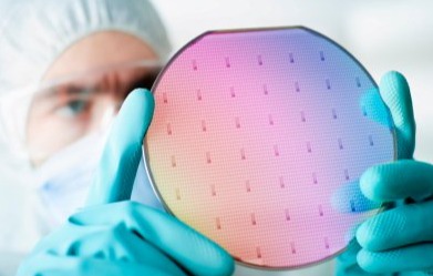
Creating a semiconductor device on a silicon wafer is a wildly complicated and expensive process. For the most part, each step needs to be done with the utmost care in order to ensure proper device performance at the end of the cycle. Wherever that device is going to be used, your car, your phone, your dishwasher, it has to work just like it was designed. In order to achieve that, semiconductor processing takes place in a clean environment (little-to-no particulate) and in equipment under low vacuum conditions (very few gas molecules). Even with all that care given to the environment, problems can occur. Modern fabrication processes have moved towards using more and harsher chemistries which can attack the equipment and lead to costly failures and downtime.
Minimizing those failures is one area where SilcoTek coatings have helped!
There are largely six ‘key’ processes in modern device manufacturing – etch, photoresist, lithography, ionization, deposition, and packaging. SilcoTek coatings were first adopted as protective layers in gas delivery for corrosive etch gases. The environment upstream from an etch processing chamber is typically controlled and under vacuum. Over time, though, the various chemistries (often halogens) used to remove material on the device wafers will also corrode the stainless steel piping, introducing particulate and metal contamination. Through the use of a protective barrier coating, such as Silcolloy, the interaction of those nasty process gases with the steel components is reduced leading to longer equipment lifetimes and longer time between failures due to corrosion!
Last year, we reported on work that we did in conjunction with Samsung Austin which was published at SEMI’s annual Advanced Semiconductor Manufacturing Conference (ASMC) in Saratoga Springs, New York. Samsung Austin employed SilcoTek coatings in the etch system exhaust gas stream to reduce (and in some cases eliminate) corrosion of Inconel parts due to the interaction of fluorine waste gases with the environment. Samsung showed that the coated parts employed in their scrubber fleet lasted over 3 times as long as uncoated parts exposed to the same chemistry. Samsung reported that this would result in both a significant financial savings for them as well as an environmental benefit by reducing their metal and solid waste streams.
Using SilcoTek solutions on both sides of the etch processing chambers has been a success, so what are some of the other challenging environments where a coating could help?
If we stick with what we know, deposition processes would be a natural next step. Many of those corrosive etch gases are used as cleaning chemistries in the deposition chambers. Metal hydrides and metal halides are also some of the original deposition precursors favored by the industry for their volatility in process yet stability in storage. While several of these compounds have been replaced as precursors by metal-organic substitutes for chemical vapor deposition (CVD) or atomic layer deposition (ALD) processes, some have not and those metal halide chemistries can prove challenging.
Metal halides will naturally break down to produce halogen gases or they can react with moisture to create acids which can, of course, corrode the metals in the process stream. Similar to the success of SilcoTek coatings in etch gas delivery, the barrier coating can be employed to help. In fact, SilcoTek’s Dursan coating (a functionalized silicon oxide layer) can serve a dual purpose as a barrier to interactions between the metal halide and the stainless steel as well as a hydrophobic barrier to moisture adsorption during installation and maintenance.
Help us help you!
SilcoTek is actively looking for partners who want to help prove this solution in the semiconductor manufacturing environment as some of the specific testing isn’t commercially available. If you’d like to learn more about our Semiconductor solutions or talk to us about setting up a test on your equipment, please contact us for options.

